Sunday 13 August 2023

How do you decide best Floorplan in Physical Design?

 Designing the best floorplan in physical design is a crucial step in integrated circuit (IC) design, as it can significantly impact the overall performance, power consumption, and manufacturability of the chip. A floorplan determines the placement of various functional blocks, standard cells, and other components on the chip's silicon area. Here are the key considerations and steps involved in deciding the best floorplan:

1. Block Placement:

   - Identify the different functional blocks, such as CPUs, memory, I/O, and custom blocks, that need to be placed on the chip.

   - Consider the block sizes, aspect ratios, and power/thermal requirements of each block.

2. Hierarchy and Partitioning:

   - Determine if a hierarchical floorplan is necessary, where blocks are grouped and placed at different levels of the hierarchy.

   - Partition the design into logical regions or modules based on functional requirements.

3. Power and Signal Integrity:

   - Place power-hungry blocks and components near the power supply to minimize voltage drop.

   - Place critical blocks closer to I/O interfaces to reduce signal propagation delays and ensure signal integrity.

4. Clock Tree:

   - Plan the clock tree distribution network and place clock sources (oscillators, PLLs) strategically to minimize clock skew and power consumption.

5. Noise and Interference:

   - Consider minimizing the coupling of noisy blocks (e.g., clock generators) with sensitive analog or RF blocks.

   - Place noisy or high-frequency blocks away from critical signal paths to avoid interference.

6. Routing and Wirelength:

   - Plan the floorplan to minimize wirelength between blocks, which reduces signal delay and power consumption.

   - Arrange blocks such that the interconnects between them are short and manageable.

7. Heat Dissipation:

   - Distribute heat-generating blocks to avoid localized hotspots. Place power-hungry blocks near heat sinks or cooling mechanisms.

8. Symmetry and Regularity:

   - Use symmetry and regularity in floorplan design to simplify routing and achieve balanced performance across different regions.

9. Design Rules and DRC:

   - Adhere to design rules and design rule checks (DRC) to ensure manufacturability. Place blocks considering metal pitch, spacing, and other lithographic constraints.

10. Iterative Refinement:

    - Floorplanning is often an iterative process. Use floorplanning tools to experiment with different arrangements and assess the impact on performance metrics.

11. Tool-Driven Optimization:

    - Utilize advanced floorplanning tools that employ optimization algorithms to automatically generate or refine floorplans based on specified objectives.

12. Trade-offs and Metrics:

    - Define design objectives and metrics such as performance, power, area, and signal integrity. Make trade-offs between these metrics to achieve the best compromise.

13. Consulting Experts:

    - Collaborate with experienced physical design engineers, as their insights can help you make informed decisions based on the specifics of the design.
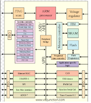


System on Chip (SoC)

A System on Chip (SoC) in VLSI (Very Large Scale Integration) design refers to the integration of multiple functional components or subsystems of an electronic system onto a single integrated circuit (IC) chip. SoC design aims to consolidate various hardware and sometimes software elements that traditionally existed as separate chips or components onto a single chip, resulting in reduced size, cost, and power consumption, while often enhancing performance and integration.

Key characteristics and aspects of SoC VLSI design include:

1. Integration of Functional Blocks: SoCs integrate different functional blocks such as processors (CPU, GPU, DSP), memory subsystems, I/O interfaces, digital and analog peripherals, communication interfaces (Wi-Fi, Bluetooth, Ethernet), and more.

2. Complexity:  SoCs are highly complex and may involve billions of transistors due to the integration of diverse functionalities.

3. Interconnect Fabric: A sophisticated interconnect fabric is required to enable communication between the various components on the chip.

4. Power Management: SoCs typically employ advanced power management techniques to optimize energy consumption by selectively powering down or adjusting voltage/frequency of different blocks.

5. Design Hierarchy: SoC design often follows a hierarchical approach, with subsystems designed and verified separately before integrating them into the final chip.

6. Verification and Validation: Due to the complexity, verification and validation of a SoC design is a significant challenge, involving simulation, emulation, and formal methods.

7. IP Cores and Reuse: SoC design often involves using pre-designed intellectual property (IP) cores for standard functions, which allows for faster development and reduces design risk.

8. Embedded Software: SoCs typically include embedded software to control and manage the hardware components, necessitating a close synergy between hardware and software design.

9.  Application Areas: SoCs find applications in a wide range of fields, including consumer electronics (smartphones, tablets), automotive (infotainment systems, autonomous driving), industrial automation, IoT devices, medical devices, and more.

10.  Design Challenges: SoC VLSI design comes with challenges like ensuring proper timing, signal integrity, thermal management, power delivery, and addressing the trade-offs between performance, power consumption, and area.

11. Customization: Some SoCs are designed for specific applications and can be customized to meet the unique requirements of that application.

12.  Advances in Technology: As semiconductor manufacturing technology advances, SoCs become more powerful and energy-efficient, enabling the development of increasingly sophisticated and capable devices.


Fig :: Example of SoC


Saturday 15 April 2023

SDC Constraint File

 An SDC (Synopsys Design Constraints) file is a text file that contains timing constraints for a digital design. The SDC file is used by the synthesis tool, place and route tool, and timing analysis tool to ensure that the design meets its timing requirements.


Here are some of the key items that can be found in an SDC constraint file:


Clock constraints: The SDC file contains information about the clock signals used in the design, including their frequency, period, and waveform characteristics. It also includes information about clock networks, such as clock tree synthesis (CTS) constraints and clock domain crossings (CDC) constraints.


Timing constraints: The SDC file contains timing constraints that define the timing relationships between signals in the design. These include setup and hold times, recovery and removal times, and minimum and maximum delays.


Constraints on input and output ports: The SDC file contains information about input and output ports of the design, including timing requirements such as input delay, output delay, and maximum fanout.


Physical constraints: The SDC file contains physical constraints such as placement constraints, routing constraints, and constraints on the timing characteristics of specific paths or cells.


Design requirements: The SDC file also contains information about the design requirements, such as power consumption constraints, design for test (DFT) constraints, and design for manufacturability (DFM) constraints.

What is follow pin in VLSI physical design?

 In VLSI physical design, a follow pin is a special type of pin used to specify the routing direction of a net or signal. The follow pin is used to guide the routing of a net, making sure that it follows a specific direction or path.

Follow pins are often used in high-speed digital circuits, where the routing of signals can significantly affect the performance of the circuit. Designers may ensure that the signal takes the best path by setting the routing direction of a net using a follow pin, lowering the chance of crosstalk and other problems. It often sits at the start or end of a net and specifies which way the signal should be sent. The signal is then routed along the designated path using the pins attached to the net, ensuring that it travels in the intended direction. To further boost the performance of the circuit, follow pins can be utilised in conjunction with other routing strategies like wire spacing and shielding. In summary, a follow pin is a special type of pin used in VLSI physical design to specify the routing direction of a net or signal. It is used to guide the routing of a net, ensuring that the signal follows the optimal path and reducing the risk of crosstalk and other issues. Follow pins are particularly useful in high-speed digital circuits, where signal routing can significantly affect circuit performance.

Crosstalk in Physical Design

 What is crosstalk?

Crosstalk in physical design is an unwanted signal coupling happens between two or more signal which are very close to each other. Crosstalk causes interference in signal because of which signal integrity of the signal gets hampered. crosstalk also degrades the performance of the circuit. How Crosstalk Occurs? it happens because of electromagnetic field generated by the signal which are transmitted through wires that are close to each other, the electromagnetic field generated by one wire can couple with the adjacent wires, causing interference. This interference can lead to signal distortion, timing errors, and noise, which can ultimately affect the performance of the circuit. How to reduce crosstalk? Crosstalk is a very common issue in while designing electronic circuit, It is more prominent while designing high speed circuit and high frequency circuit. There are various ways used designers to reduce crosstalk such as wire spacing :: Wire spacing involves placing the wires at a distance from each other, which reduces the electromagnetic coupling between them. shielding :: Shielding involves adding a metallic layer between the wires, which reduces the interference caused by the electromagnetic fields differential signaling :: Differential signaling involves transmitting signals on two wires that have equal but opposite voltages. This cancels out the effects of crosstalk. There are others ways also reduce crosstalk such as buffering the net, strengthen the driver cells of victim net etc.

Difference Between 7nm and 14nm process nodes

1. Definition of Process Node

Process node refers to the size of the transistors and other components on chip.

Process node is measured in nanometers.

As size of process node is decreases, it will allow more number transistor to be packed onto single chip. It will result in higher performance and low power consumption

2. 7nm Vs 14nm Process Nodes

The 7nm process has smaller transistors compared to the 14nm process, allowing more transistors to be packed into a smaller area on the IC.

The smaller transistors mean better performance and lower power consumption because they can switch faster and require less energy.

The 7nm process uses a FinFET (Fin Field-Effect Transistor) architecture that provides better control over the channel, reducing leakage current and improving overall performance.

The FinFET architecture also allows for better scalability, enabling further increases in transistor density.

3. Advantages of the 7nm Process Node

Higher performance: The smaller size of transistors in the 7nm process allows for faster switching and better overall performance.

Lower power consumption: The smaller transistors require less energy to switch, resulting in lower power consumption and longer battery life in devices.

Better control over the channel: The FinFET architecture used in the 7nm process provides better control over the channel, reducing leakage current and improving overall performance.

Improved scalability: The FinFET architecture also allows for better scalability, enabling further increases in transistor density.

4. Challenges of the 7nm Process Node

Increased complexity: The 7nm process requires multiple patterning, EUV (Extreme Ultraviolet) lithography, and complex multi-layered stacks, making the manufacturing process more complex and expensive.

Reduced yield: With the smaller size of transistors, the number of defects per wafer increases, making it harder to produce functional chips. This has resulted in increased costs, as manufacturers need to produce more wafers to achieve the same yield as previous generations.

5. Cost-Effective Solutions for the 7nm Process Node

Multi-chip modules: Instead of producing a single large chip, manufacturers can produce smaller chips and combine them to create larger, more complex systems.

Chiplet architectures: This approach breaks down the chip into smaller, more manageable pieces or chiplets, which can then be integrated into a larger system-on-a-chip (SoC).

These solutions can help mitigate the challenges of the 7nm process and provide a more cost-effective way to produce high-performance ICs.


As process node come down from 14 nm to 7nm size of transistor has become smaller, which provides good performance and lower power consumption. In smaller process nodes manufacturing of chips becomes complex, which may result in yield reduction. 


Thursday 9 February 2023

"Comparing ASIC and FPGA: Understanding the Key Differences"

 FPGA (Field-Programmable Gate Array) and ASIC (Application-Specific Integrated Circuit) are two popular choices in digital integrated circuit design. The key differences between the two are as follows:

Flexibility: FPGAs are highly flexible as they can be programmed to perform a wide range of digital functions. On the other hand, ASICs are designed specifically for a particular application and cannot be reprogrammed.

Time-to-Market: FPGAs typically have a shorter time-to-market than ASICs as they can be quickly configured and tested. ASICs, on the other hand, require a longer design cycle, including tapeout and fabrication.

Cost: FPGAs are typically more expensive than ASICs for low volume applications, but the cost per unit decreases as volume increases. ASICs are more cost-effective for high-volume applications.

Power Consumption: ASICs typically consume less power than FPGAs, but the power consumption of FPGAs can be reduced through power-saving techniques.

Performance: ASICs can deliver higher performance than FPGAs as they are optimized for a specific application. FPGAs, on the other hand, are more general-purpose and may not provide the same level of performance for a specific application.

In conclusion, the choice between FPGA and ASIC depends on the specific requirements of the application, including flexibility, time-to-market, cost, power consumption, and performance.

Computation of Target IR Drop Value

 IR drop is the voltage drop that occurs in the power distribution network due to the resistance and inductance of the interconnects and packages. In physical design, the target IR drop value is a desired value that is set to ensure the reliability and performance of the circuit.

To compute the target IR drop value in the core from the target IR drop value, the following steps can be followed:

Determine the target voltage drop: The target IR drop value is specified as a voltage drop across the power distribution network. The target voltage drop can be determined by subtracting the desired supply voltage from the nominal voltage of the power distribution network.

Determine the power density: The power density of the core can be estimated based on the power consumption of the circuit and the area of the core.

Estimate the resistance and inductance: The resistance and inductance of the power distribution network can be estimated based on the interconnect metal stack and the package parasitics.

Calculate the current: The current in the power distribution network can be calculated based on the power density and the voltage drop.

Calculate the target IR drop: The target IR drop value can be calculated by multiplying the current by the resistance and inductance of the power distribution network.

By computing the target IR drop value in the core from the target IR drop value, the power distribution network can be designed to meet the desired performance and reliability requirements.

Methods to Reduce Dynamic Power Consumption in IC

 Dynamic power consumption is the power consumed by digital circuits during switching events. In physical design, there are several techniques that can be used to reduce dynamic power consumption:

Clock gating: This technique involves stopping the clock signal to blocks of the circuit that are not in use, reducing the Clock gating: dynamic power consumption.

Power gating: This technique involves turning off the power supply to blocks of the circuit that are not in use, reducing the overall power consumption, including dynamic power.

Voltage scaling: This technique involves reducing the operating voltage of the circuit to reduce its power consumption, including dynamic power.

Input vector control: This technique involves controlling the input vectors to reduce the number of switching events and thereby reduce the dynamic power consumption of the circuit.

Power-aware placement and routing: This technique involves optimizing the placement and routing of the circuit to reduce the power consumption, including dynamic power.

Power-aware synthesis: This technique involves optimizing the logic synthesis of the circuit to reduce the power consumption, including dynamic power.

Power-aware testing: This technique involves optimizing the testing of the circuit to reduce the power consumption, including dynamic power.

Multi-Vt cell libraries: This technique involves using cells with different threshold voltages in the design to reduce the dynamic power consumption by reducing the switching activity.

By using a combination of these techniques, significant reductions in dynamic power consumption can be achieved in physical design.

Input Vector Control and Leakage Reduction

 Input vector control and leakage reduction are two important techniques used in physical design to reduce power consumption and improve the energy efficiency of digital circuits.

Input Vector Control: Input vector control is a low power technique that involves controlling the input vectors to reduce the number of switching events and thereby reduce the dynamic power consumption of the circuit. This is achieved by controlling the inputs to the circuit such that the switching activity is reduced, resulting in lower dynamic power consumption.

Leakage Reduction: Leakage power is the power that is consumed even when the circuit is not actively switching. Leakage reduction techniques aim to minimize this power consumption. Some common leakage reduction techniques are:

Threshold voltage adjustment: The threshold voltage of the transistors in the circuit can be adjusted to reduce the leakage current and thereby reduce the leakage power.

Dual Vt cell libraries: The use of cells with two threshold voltages can reduce the leakage power by using high-threshold transistors for the leakage-sensitive portions of the circuit.

Power gating: This technique involves turning off the power supply to blocks of the circuit that are not in use, reducing the overall power consumption, including leakage power.

Body biasing: This technique involves biasing the body of the transistors in the circuit to control the leakage current and reduce the leakage power.

By combining input vector control and leakage reduction techniques, significant reductions in power consumption can be achieved in physical design.

Low Power Design Techniques Used in Physical Design


Low power design techniques are used in physical design to minimize the power consumption of digital circuits and systems. The objective of low power design is to reduce the power dissipation while maintaining or improving the circuit performance. Some of the common low power techniques used in physical design are:

Power gating: This technique involves turning off the power supply to blocks of the circuit that are not in use, reducing the overall power consumption.

Clock gating: This technique involves stopping the clock signal to blocks of the circuit that are not in use, reducing the dynamic power consumption.

Voltage scaling: This technique involves reducing the operating voltage of the circuit to reduce its power consumption.

Multi-Vt cell libraries: This technique involves using cells with different threshold voltages in the design to reduce the power consumption.

Power-aware placement and routing: This technique involves optimizing the placement and routing of the circuit to reduce the power consumption.

Power-aware floorplanning: This technique involves optimizing the floorplan of the circuit to reduce the power consumption.

Power-aware synthesis: This technique involves optimizing the logic synthesis of the circuit to reduce the power consumption.

Power-aware testing: This technique involves optimizing the testing of the circuit to reduce the power consumption.

These techniques can be used in combination to achieve a significant reduction in power consumption in physical design.

Why is the NAND gate more widely utilized than the NOR gate in digital logic circuits?

 The NAND gate is more widely utilized than the NOR gate in digital logic circuits due to several factors, including:

Universal Gates: NAND gates can be used to implement any other type of logic gate, such as AND, OR, NOT, and XOR gates. This universality makes NAND gates more versatile and easier to use in digital logic circuits.

Improved Performance: NAND gates have faster switching times and consume less power compared to NOR gates. This makes NAND gates more suitable for high-speed and low-power digital logic circuits.

Lower Cost: NAND gates are easier to fabricate, test and integrate into digital circuits, which makes them less expensive compared to NOR gates.

Industry Standard: NAND gates have been widely adopted as the standard in the digital logic industry, which has further contributed to their popularity over NOR gates.

All these factors have made NAND gates preferred over NOR gates in digital logic circuits.

Cell placement


Cell placement is a key step in the VLSI (Very Large Scale Integration) Physical Design process. It involves determining the physical location of each component, such as transistors, capacitors, and resistors, on the chip. The goal of cell placement is to create a design that meets the performance and reliability requirements while also optimizing the utilization of the chip area.


Cell placement is a complex process that involves considering several factors, including:

1.       Performance: The performance of the chip is affected by the placement of components, the routing of metal lines, and the distribution of power and ground. It is important to optimize the placement of components to meet the performance requirements.

2.       Power Consumption: The placement of components and the routing of power and ground lines can impact the chip's power consumption. It is important to optimize the placement of components to minimize power consumption.

3.       Area Utilization: The utilization of the chip area is an important factor, as it affects the cost of the chip. It is important to optimize the utilization of the chip area while also meeting the performance and power consumption requirements.

4.       Design Rules: The design rules define the minimum and maximum distances between components and metal lines, as well as the minimum widths and spacing of metal lines. These rules must be followed to ensure that the design can be fabricated without issues.

Cell placement is typically performed using specialized software tools that use algorithms to optimize the placement of components. These tools consider the factors mentioned above and perform several iterations to refine the placement of components.

In conclusion, cell placement is a critical step in the VLSI Physical Design process that involves determining the physical location of each component on the chip. It involves considering several factors, including performance, power consumption, area utilization, and design rules, to create a design that meets the requirements and can be fabricated without issues.

Layout Planning

 Layout planning is critical in the VLSI (Very Large Scale Integration) Physical Design process. It involves determining the placement of components on the chip and ensuring that the chip area is optimized for maximum utilization. The goal of layout planning is to create a design that meets the performance and reliability requirements while also optimizing the utilization of the chip area.

Layout planning is a complex process that requires a deep understanding of the design, the manufacturing process, and the design rules. It is important to balance the trade-offs between performance, power consumption, and area utilization and consider the interactions between different components on the chip.

There are several factors to consider during layout planning, including:


1. Design Rules: The design rules define the minimum and maximum distances between components and metal lines, as well as the minimum widths and spacing of metal lines. These rules are set by the manufacturing process and must be followed to ensure that the design can be fabricated without issues.

2. Performance: The performance of the chip is affected by the placement of components, the routing of metal lines, and the distribution of power and ground. It is important to optimize the placement of components and the routing of metal lines to meet the performance requirements.

3. Power Consumption: The placement of components and the routing of power and ground lines can impact the chip's power consumption. It is important to optimize the placement of components and the routing of power and ground lines to minimize power consumption.

4. Area Utilization: The utilization of the chip area is an important factor, as it affects the cost of the chip. It is important to optimize the utilization of the chip area while also meeting the performance, power consumption, and design rule requirements.


Layout planning is an iterative process that involves several iterations to refine the placement of components and the routing of metal lines. It requires close collaboration between the design and manufacturing teams to ensure that the design meets the requirements and can be fabricated without issues.

In conclusion, layout planning is a critical step in the VLSI Physical Design process that involves determining the placement of components on the chip and ensuring that the chip area is optimized for maximum utilization. It requires a deep understanding of the design, the manufacturing process, and the design rules, as well as a balance of trade-offs between performance, power consumption, and area utilization.