Sunday 5 March 2017

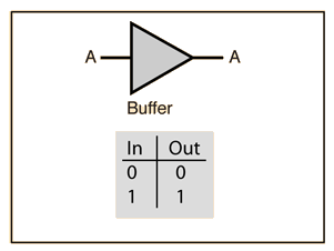
Buffer

digital buffer (or a voltage buffer) is an electronic circuit element that is used to isolate the input from the output, providing either no voltage or a voltage that is same as the input voltage. It draws very little current and will not disturb the original circuit. It is also called as unity gain buffer or a because it provides a gain of 1, which means it provides at most the same voltage as the input voltage, serving no amplification function.

Image result for buffer in vlsi


Usage of buffer in Physical Design

1. Setup Violation fixes
2. Hold Violation fixes
3. Max Trans Violation Fixes
4. xtalk reduction


Inrush Current

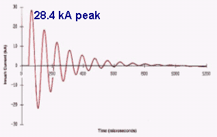
Inrush currentinput surge current or switch-on surge is the maximum, instantaneous input current drawn by an electrical device when first turned on. Alternating current electric motors and transformers may draw several times their normal full-load current when first energized, for a few cycles of the input waveform. Power converters also often have inrush currents much higher than their steady state currents, due to the charging current of the input capacitance. The selection of overcurrent protection devices such as fuses and circuit breakers is made more complicated when high inrush currents must be tolerated. The overcurrent protection must react quickly to overload or short circuit faults but must not interrupt the circuit when the (usually harmless) inrush current flows.


How to calculate Inrush Current?


Source:- Wikipedia


Sunday 19 February 2017

How to fix max trans violation?

 There are several ways to fix the transition time violations.

1) Increase the driver size.
2) Break the nets in the case of long nets.
3) Break the large fanout by duplicating drivers or with buffering.
4) Change the VT if option available(changing drivers from hvt to svt or lvt).
5) Reduce the load by downsizing the cells(special cases) after the looking the timing impact on the design.
6) Change the Load to hvt because hvt has higher lib limit.

Friday 17 February 2017

Physical design Interview Question part 8

What are well tap cells, what are end cap cells and its usage
What are the inputs to CTS
What sanity checks are to be done in SDC file
What is de-rating
What is clock skewing and what is a useful skew
how many clocks are used in your project
what is the maximum frequency
what is latency
what is clock generation point, clock distribution point, clock end point
why is the setup check in next cycle and hold checked at same time
what is the width and spacing rules for clocks
what are the NDR for clocks
what are NDR and DRC checks done at each stage of project
what is OCV, antenna violation and what are measures taken
what is antenna ratio
what is RC extraction and when do you do this
if you have congestion after CTS and you are not allowed to change the placement how do you proceed
does set up fixes cause hold issues and vice versa
what is slack
what happens if there is any floating pin and it is left without any care
what is electro migration
what is signal integrity and cross talk
what are the preventions taken at each stage to resolve cross talk issue
what is shielding
what is Physical verification, formal verification
what are the DRC checks made in project
what is LVS what information is obtained from LVS
what are the signoff checks and which tools are used for it
what are the inputs to STAR RC and prime time
what is cloning
what happens if any of the input files are missed to IC compiler
what is RTL , gate level differences
What does synthesis team do?
What are libraries needed for tool, what is difference between logic and physical library
What is a UPF file, is it used in your project
What ae filler cells
What are ECOs , how many Eco are implemented
What ae the DRC fixed
What is low power design
What is clock and power gating

Physical Design Interview Part 7

Tell me about yourself in brief
Inputs to PNR
Do you have knowledge on synthesis
What are the validations and sanity checks you do on the outputs received from synthesis team
Which file will you need to check if you see black box in the screen
Which file you need to check if you see any floating pins and whom should you report in such case
What does .tf file, .db file, .sdc file, .spef file .v files include
What is floor plan and what is done as part of floor plan
How do you fix placement of RAMs 
What is utilization factor and Area
What is fly line analysis
How do you decide the spacing between the macros and standard cells
What are tie cells and can the size of array of tie cells be either increased or decreased? –No
Which layers are preferred for power routing and why?
Which is preferred to be the outer most layer or top layer
What is the UF in floor plan
What is the skew achieved in your project and what is the allowed skew
What is local skew and global skew difference
What are the tools used for PNR
What is high fan out synthesis
What is placement and what do we do in this step
What is NLDM
What is congestion and timing closure
What special physical cells are used  in your project
Purpose of power domains, level shifter cells, isolation cells, Always on cell
Where do we use Always On buffers
How is drive strength and delay relation
What is inversion temperature
How is delay and temperature relation
How is threshold voltage and temperature variations related
What happens when you do congestion driven placement
Where are the buffers placed? What is the functionality of buffers
How do buffers speed up the signal in data or in clock even if it adds delay to the path
What is set up and hold violation
What are the ways to fix the set up violation
Ways to fix hold violation
What is STA and which tool is being used for STA
What are the optimizations done in placement stage
What are the power domains in your project
What is switchable power domain

Sunday 12 February 2017

Job Description: Senior ASIC Design Engineer (Physical Design)

In this position, the individual will be responsible for driving Place-And-Route flow for Low Power Designs from netlist to GDS. Responsibilities will include complete ownership of sub chip PnR environment, clock tree design and driving Place-And-Route flow for full chip convergence and timing closer.
This position requires a Master’s Degree in Electrical Engineering or Computer Science with a minimum of 4 to 7 years of hands on experience in sub chip Place-And-Route flow with emphasis on 28nm and low power designs. Proficiency in SoC Encounter / Innovus / ICC / ICC II and experience in PERL/TCL/Shell scripting is a must.  
The individual must have hands on experience with multiple low power hierarchical and flat ASICs at 28 nm and below nodes. Having exposure to Physical Verification flow for DRC and LVS closure for blocks is preferred. Ability to work with minimal supervision and drive to exceed expectations is a must.  Good verbal and written communication skills are required.

Details required:
Total Experience:
Relevant Experience:
Current CTC (Fixed & Variable):
Expected CTC:
 Notice Period:
Any offers in hand:
Job Location: Noida, Bangalore
Have you applied for this company past 6 months:
Looking forward to be of assistance to you.
Kindly revert back with your interest and Updated CV @vlsijunction@gmail.com

Tuesday 17 January 2017

STA Interview Question Part 5

1)what are inputs for Prime Time?

2)Explain the Prime time inputs?

3)Analyze the Timing Report?

4)what is Setup time? Draw the waveforms ?

5)what you have done in your Projects?(About Timing)

6)what is Arrival time,Required Time?

7)what .lib, .spef contains ?

8)what is Timing Window?

9)why Setup time and Hold time ?

10)In a file, it contains lot of linked file paths there Replace the .lef extension with .txt

11)A file contains a few No. of lines there , show the memory of the Each line in Terminal?

12)Open a tcl file and Copy the Data and paste into another file?

13)Show the a file information in screen?(in Tclsh shell)

14)Search patterens in Vi file?