Showing posts sorted by relevance for query physical verification. Sort by date Show all posts

Saturday, 8 August 2015

Physical Verification

Physical Verification Introduction
After routing, your layout is complete. Now a number of checks are performed to verify that the drawn layout works as intended.
  1. Physical verification
  2. Equivalence Checking
  3. Timing Analysis
Equivalence check will compare the netlist we started out with (pre-layout/synthesis netlist) to the netlist written out by the tool after PnR(postlayout netlist).Physical verification will verify that the post-layout netlist and the layout are equivalent. i.e. all connections specified in the netlist is present in the layout.This article explains physical verification.
Physical Verification
After routing, your PnR tool should give you zero DRC/LVS violations. However, the PnR tool deals with abstracts like FRAM or LEF views. We use dedicated physical verification tools for signoff LVS and DRC checks. Some of these are Hercules from Synopsys, Assura from Cadence and Calibre from MentorGraphics.
The major checks are:
  1. DRC
    DRC checks determine if the layout satisfies a set of rules required for manufacturing. The most common of these are spacing rules between metals, minimum width rules, via rules etc.There will also be specific rules pertaining to your technology. An input to the design rule tool is a ‘design rule file’ (called a runset by Synopsys’ hercules). The design rules ensure sufficient margins to correctly define the geometries without any connectivity issues due to proximity in the semiconductor manufacturing processes, so as to ensure that most of the parts work correctly. The minumum width rules exists for all mask layers, and spacing between the same layers are also specified. Spacing rules may change depending on the width of one or both of the layers as well. There can also be rules between two different layers, and specific via density rules etc. If the design rules are violated, the chip may not be functional.
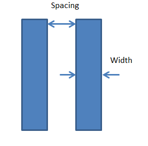
    Spacing & Width checks
    DRC – Spacing & Width checks
    DRC checking software, like Assura, Hercules or Calibre usually takes the layout in any of the supported formats, like GDSII.
  2. LVS
    LVS is another major check in the physical verification stage. Here you are verifying that the layout you have created is functionally the same as the schematic/netlist of the design-that you have correctly transferred into geometries your intent while creating the design. So all the connections should be proper and there shouldn’t any missing connections etc.
    The LVS tool creates a layout netlist, by extracting the geometries. This layout netlist is compared with the schematic netlist. The tool may require some steps to create either of these netlists(e.g. nettran run in synopsys)
    If the two netlists match, we get an LVS clean result. Else the tool reports the mismatch and the component and location of the mismatch. Along with formal verification, which verifies if your pre-layout netlist matches the post-layout netlist,LVS verifies the correctness of the layout w.r.t intended functionality.
    Some of the LVS errors are:
    • Shorts – Wires that should not be connected are overlapping.
    • Opens – Connections are not complete for certain nets.
    • Parameter mismatch – LVS also checks for parameter mismatches. e.g. It may match a resistor in both layout and schematic, but the resistor values may be different. This will be reported as a parameter mismatch.
    • Unbound pins – If the pins don’t have a geometry, but all the connection to the net are made, and unbound pin is reported.
  3. Antenna
  4. Process antenna effect or “plasma induced gate oxide damage” is a manufacturing effect. i.e. this is a type of failure that can occur solely at the manufacturing stage. This is a gate damage that can occur due to charge accumulation on metals and discharge to a gate through gate oxide.
    Let us see how this happens. In the manufacturing process, metals are built layer by layer. i.e. metal1 is deposited first, then all unwanted portions are etched away, with plasma etching. The metal geometries when they are exposed to plasma can collect charge from it. Once metal1 is completed, via1 is built, then metal2 and so on. So with each passing stage, the metal geometries can build up static electricity. The larger the metal area that is exposed to the plasma, the more charge they can collect. If the charge collected is large enough to cause current to flow to the gate, this can cause damage to the gate oxide. This happens because since the layers are built one-by-one, a source/drain implant may not be available for discharge as in fig.b.
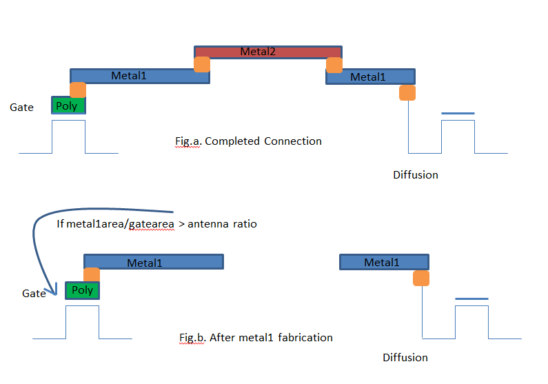
    Process Antenna
    Process Antenna
    Antenna rules are normally expressed as an allowable ratio of metal area to gate area. Each foundry sets a maximum allowable antenna ratio for its processes. If the metal area–which is cumulative, i.e. the sum of the ratios of all lower layer interconnects in addition to the layer in check–is greater than the allowable area, the physical verification tool flags an error.For example, let’s say maximum allowable antenna ratio for metal1 is 400. If the gate area is 1 sq.u and if the metal area connecting to the gate is 500 sq.u, there will be a process antenna violation.
  5. ERC
    ERC (Electrical rule check) involves checking a design for all electrical connections that are considered dangerous.
    • Floating gate error – If any gate is unconnected, this could lead to leakage issues.
    • VDD/VSS errors – The well geometries need to be connected to power/Ground and if the PG connection is not complete or if the pins are not defined, the whole layout can report errors like “NWELL not connected to VDD.

You may be also interested in below topics

Tuesday, 27 December 2016

Physical design Interview Questions Part 6

Below are interview questions asked by one of the product based company

1. Have you ever worked on on lower nodes, like 14nm or 10nm?
2. what is difference between bulk MOS and FINFET?
3. How conduction takes place in MOS and FINFET transistors?
4. Is Antennae violation is functional failure or Manufacturing error? how can you fix antennae               violation
5. What is short circuit current, and how will you overcome this problem?
6. What is difference between static IR drop and dynamic IR drop?
7. On what all parameters does IR drop and Dynamic IR drop depends on?
8. Have you worked on Physical Verification?
9. What is soft checks in Physical verification?
10. How soft checks different from ERC?
11. What is difference between ERC and PERC?
12. What all the Physical verification test you perform during each stage of Physical design?
13. what XOR checks will do?
14. have you ever worked in STA?
15. have you involved in top level timing or your role limited to block level timing?

16. How OCV (onchip variation diffrent from ) AOCV (advance on chip variation)?
17 what is difference between  AOCV and POCV?
18 how timing related with PTC (postive temperature coefficient) and NTC (negative              temperature coefficient)
19 how derates varies in ocv, aocv and pocv?
20. what all parameter of uncertainty value in STA depends upon pre cts and post cts 

Thursday, 22 October 2015

Physical Design Course for beginners

Detailed list of Topics, Note this topics will be timely updated as per requirement, any feedback and suggestions are welcome (please write on comment section or send mail us to vlsijunction@gmail.com)


PreRequisite


FloorPlannig topics


STA


Sign Off Check


DFM


Tools Guide and References


Interview Questions

Physcial Design

Career In Physical Design


References


Thursday, 20 August 2015

Physical Design Flow

Physical Design Flow


In integrated circuit design, physical design is a step in the standard design cycle which follows after the circuit design. At this step, circuit representations of the components (devices and interconnects) of the design are converted into geometric representations of shapes which, when manufactured in the corresponding layers of materials, will ensure the required functioning of the components. This geometric representation is called integrated circuit layout. This step is usually split into several sub-steps, which include both design and verification and validation of the layout.

Modern day Integrated Circuit (IC) design is split up into Front-end design using HDL's, Verification and Back-end Design or Physical Design. The next step after Physical Design is the Manufacturing process or Fabrication Process that is done in the Wafer Fabrication Houses. Fab-houses fabricate designs onto silicon dies which are then packaged into ICs.
Each of the phases mentioned above have Design Flows associated with them. These Design Flows lay down the process and guide-lines/framework for that phase. Physical Design flow uses the technology libraries that are provided by the fabrication houses. These technology files provide information regarding the type of Silicon wafer used, the standard-cells used, the layout rules, etc.
Technologies are commonly classified according to minimal feature size. Standard sizes, in the order of miniaturization, are 2μm, 1μm , 0.5μm , 0.35μm, 0.25μm, 180nm, 130nm, 90nm, 65nm, 45nm, 28nm, 22nm, 18nm... They may be also classified according to major manufacturing approaches: n-Well process, twin-well process, SOI process, etc.
The main steps in the flow are:

  • Design Netlist (after synthesis)
  • Floor Planning
  • Partitioning
  • Placement
  • Clock-tree Synthesis (CTS)
  • Routing
  • Physical Verification
  • GDS II Generation


These steps are just the basic. There are detailed PD Flows that are used depending on the Tools used and the methodology/technology. Some of the tools/software used in the back-end design are :
  • Cadence (SOC Encounter, VoltageStorm, NanoRoute)
  • Synopsys (Design Compiler, IC Compiler, PrimeTime)
  • Magma (BlastFusion, Talus )
  • Mentor Graphics (Olympus SoC, IC-Station, Calibre)     
 
 
You May also interested  in Below topics 

Scripts used in IC Compiler
Basics of IC Compiler

Saturday, 20 February 2016

Physical Design Interview Question Part 1


  1. Explain concept of   cross talk? 
  2. How can you overcome cross talk problem? 
  3. what is shielding? how it avoid avoids crosstalk problem? 
  4. how spacing h reducing crosstalk noise? 
  5. Why double spacing and multiple vias are used related to clock? 
  6. where do you insert buffer to avoid crosstalk? how buffer insertion solve the problem?
  7. Difference between Chip Design and Block level design? 
  8. What are the ways to place macros in a full chip design? 
  9. what are the differences between Hierarchical Design and flat design? 
  10. Why 500 MHz clock design is complex than 48Mhz design? 
  11. What all tools used in physical verification? 
  12. what are the inputs you will give in physical verification
  13. how will you solve the congestion between two macros? 
  14. what all parameters you will consider while estimating die size? 
  15. What is each macro size and number of standard cell count? 
  16. Depends on your design. 
  17. What are the input needs for your design?  
  18. What does SDC (Synopsys design contraint)  file contains? 
  19. how will give Clock definitions ?
  20. what are timing Timing exception, how will you constraint them?
  21. what is Input and Output delays, what are prime time  commands for it?
  22. How did you do power planning? 
  23. Explain, how will you find number of power pad and IO power pads? 
  24. How the  number of power straps calculate? 
  25. How to find total power of chip, What are the problems you can  faced with respect to timing? 
  26. what is  setup and hold problem, how will you solve it?
  27. which is preferable layer for clock routing and why? 
  28. what do you mean by IR drop problem, how will you overcome by this problem? 
  29. what is  antenna effect, how does it impact the and how would you resolve antennae effect problem? 
  30. How are the PVT conditions? Describe using graph?
  31. Describe the physical design flow?
  32. what all the  and inputs and outputs for each step of physical design? 
  33. What is cell delay and net delay, how will you reduce this delays? 
  34. What are  the different timing delay models available? 
  35. What is wire load model (WLM)?  
  36. Why higher metal layers are preferred for power? 
  37. What do you mean by logic optimization techniques, how it will work?
  38. what is slack, how will you calculate slack?
  39. what are the parameters on which slack depends on?
  40. What do you mean by of negative slack, how will u make it positive?  
  41. What is EM and it effects? 
  42. What are types of routing ?  
  43. What do you mean by clock latency? what are the  types of clock latecies? 
  44. What is track assignment in routing stage? 


Tuesday, 8 January 2019

Skill Set Required for a Physical Design Engineer

As a Physical Design Engineer Market expect the following Skill set.

1. fair knowledge of physical desgn flow, Which include RTL Synthesis, Floorplanning, Placement of cells, Clock Tree Synthesis, Routing.
2. knowledge of Sign off checks like Static Timing Analysis, IR drop checks, Physical verification Checks, Logical Equivalence checks, Low Power checks
3. Scripting Languages Like Perl, TCL etc.
4. EDA Tool knowledge, Mostly tools from Synopsys and cadence are used in Physical Design.

In case of any query related to physical Design Please feel to drop an email @ vlsijunction@gmail.com

for latest post do follow our facebook page :: https://www.facebook.com/vlsijunction

Thursday, 30 May 2019

What is Physical Design?

The physical design is the process of transforming a circuit description into the physical layout, which describes the position of cells and routes for the interconnections between them. At this step, circuit representations of the components (devices and interconnects) of the design are converted into geometric representations of shapes which, when manufactured in the corresponding layers of materials, will ensure the required functioning of the components.


The main steps in the ASIC physical design flow are:

  • Design Netlist (after synthesis)
  • Floorplanning
  • Partitioning
  • Placement
  • Clock-tree Synthesis (CTS)
  • Routing
  • Physical Verification
  • GDS II Generation

Below are main sign off checks/Analysis in Physical Design

  • 1. Logical Equivalence Check
  • 2. Static Timing Analysis
  • 3. Power analysis (static and dynamic,  resistance checks etc)
  • 4. Low power Checks

Friday, 17 February 2017

Physical design Interview Question part 8

What are well tap cells, what are end cap cells and its usage
What are the inputs to CTS
What sanity checks are to be done in SDC file
What is de-rating
What is clock skewing and what is a useful skew
how many clocks are used in your project
what is the maximum frequency
what is latency
what is clock generation point, clock distribution point, clock end point
why is the setup check in next cycle and hold checked at same time
what is the width and spacing rules for clocks
what are the NDR for clocks
what are NDR and DRC checks done at each stage of project
what is OCV, antenna violation and what are measures taken
what is antenna ratio
what is RC extraction and when do you do this
if you have congestion after CTS and you are not allowed to change the placement how do you proceed
does set up fixes cause hold issues and vice versa
what is slack
what happens if there is any floating pin and it is left without any care
what is electro migration
what is signal integrity and cross talk
what are the preventions taken at each stage to resolve cross talk issue
what is shielding
what is Physical verification, formal verification
what are the DRC checks made in project
what is LVS what information is obtained from LVS
what are the signoff checks and which tools are used for it
what are the inputs to STAR RC and prime time
what is cloning
what happens if any of the input files are missed to IC compiler
what is RTL , gate level differences
What does synthesis team do?
What are libraries needed for tool, what is difference between logic and physical library
What is a UPF file, is it used in your project
What ae filler cells
What are ECOs , how many Eco are implemented
What ae the DRC fixed
What is low power design
What is clock and power gating

Friday, 7 August 2015

Important Input Files in Physical Design Flow


    1. Gatelevel Netlist

    File Format :- .v


    Provided by :- Synthesis team


    Description :- Verilog source file. Normally it’s a source file. Design Compiler, and IC Compiler can use this format for the gate-level netlist.                                                                    

    2. Physical Libraries

    File Format :- .lef (Cadence) or .CEL, .FRAM (In Synopsys)

    Provided by:- Vendor

    Description :- Library Exchange Format. Standard cells are often saved in this format. Cadence tools also often use this format. Synopsys tools normally use Milkyway format for standard cells.                                                                                                                                    

    3. Logical Libraries

    File Format :- .lib

    Provided by :- Vendor

    Description :- Technology Library source file. Technology libraries contain information about the characteristics and functions of each cell provided in a semiconductor vendor’s library. Semiconductor vendors maintain and distribute the technology libraries. In our case the vendor is Synopsys. Cell characteristics include information such as cell names, pin names, area, delay arcs, and pin loading. The technology library also defines the conditions that must be met for a functional design (for example, the maximum transition time for nets). These conditions are called design rule constraints. In addition to cell information and design rule constraints, technology libraries specify the operating conditions and wire load models specific to that technology.                                                                                                                                       

    4. Technology files

    File Format :- .techlef (Cadence) or .tf(In Synopsys)

    Provided by :- Fab House

    Description :- It describes the units, drawing patterns, layers,design rules, vias, and parasitics resistance and capacitance of the manufacturing process                                                                                                                                                                                                                         

    5. TLU+

    File Format :- .tlup

    Provided by :- Fab House

    Description :- These files are generated from the *.itf files. TLUPlus models are a set of models containing advanced process effects that can be used by the parasitic extractors in Synopsys place-and-route tools for modeling.                                                                                 

    6. Constraints Files

    File Format :- .sdc

    Provided by :- Synthesis Team

    Description :- Synopsys Design Constraints. SDC is a Tcl-based format. All commands inan SDC file conform to the Tcl syntax rules. You use an SDC file to communicate the design intent, including timing and area requirements between EDA tools. An SDC file contains the following information: SDC version, SDC units, design constraints, and comments. 


    There are different type of the files generated during a design cycle or data received by the library vendor/foundry. Few of them having specific extension. Just to know the extension, you can easily identity the type of content in that file.  


    *.ddc- Synopsys internal database format. This format is recommended by Synopsys to hand gate-level netlists.File Extensions:


    *.v- Verilog source file. Normally it’s a source file your write. Design Compiler, and IC Compiler can use this format for the gate-level netlist.


    *.vg, .g.v- Verilog gate-level netlist file. Sometimes people use these file extension to differentiate source files and gate-level netlists.


    *.svf- Automated setup file. This file helps Formality process design changes caused by other tools used in the design flow. Formality uses this file to assist the compare point matching and verification process. This information facilitates alignment of compare points in the designs that you are verifying. For each automated setup file that you load, Formality processes the content and stores the information for use during the name-based compare point matching period.


    *.vcd- Value Change Dump format. This format is used to save signal transition trace information. This format is in text format, therefore, the trace file in this format can get very large quickly. There are tools like vcd2vpd, vpd2vcd, and vcd2saif switch back and forth between different formats.


    *.vpd- VCD Plus. This is a proprietary compressed binary trace format from Synopsys. This file format is used to save signal transition trace information as well.


    *.saif- Switching Activity Interchange Format. It’s another format to save signal transition trace information. SAIF files support signals and ports for monitoring as well as constructs such as generates, enumerated types, records, array of arrays, and integers.


    *.tcl- Tool Command Language (Tcl) scripts. Tcl is used to drive Synopsys tools.


    *.sdc- Synopsys Design Constraints. SDC is a Tcl-based format. All commands in an SDC file conform to the Tcl syntax rules. You use an SDC file to communicate the design intent, including timing and area requirements between EDA tools. An SDC file contains the following information: SDC version, SDC units, design constraints, and comments. 


    *.lib- Technology Library source file. Technology libraries contain information about the characteristics and functions of each cell provided in a semiconductor vendor’s library. Semiconductor vendors maintain and distribute the technology libraries. In our case the vendor is Synopsys. Cell characteristics include information such as cell names, pin names, area, delay arcs, and pin loading. The technology library also defines the conditions that must be met for a functional design (for example, the maximum transition time for nets). These conditions are called design rule constraints. In addition to cell information and design rule constraints, technology libraries specify the operating conditions and wire load models specific to that technology.


    *.db- Technology Library. This is a compiled version of *.lib in Synopsys database format.                                                                                                                                                                *.plib- Physical Library source file. Physical libraries contain process information, and physical layout information of the cells. This information is required for floor planning, RC estimation and extraction, placement, and routing.


    *.pdb- Physical Library. This is a compiled version of *.plib in Synopsys database format.


    *.slib- Symbol Library source file. Symbol libraries contain definitions of the graphic symbols that represent library cells in the design schematics. Semiconductor vendors maintain and distribute the symbol libraries. Design Compiler uses symbol libraries to generate the design schematic. You must use Design Vision to view the design schematic. When you generate the design schematic, Design Compiler performs a one-to-one mapping of cells in the netlist to cells in the symbol library.                                                                                                                                                                                                                                                                       *.sdb- Symbol Library. This is a compiled version of *.slib in Synopsys database format.


    *.sldb- DesignWare Library. This file contains information about DesignWare libraries.


    *.def- Design Exchange Format. This format is often used in Cadence tools to represent physical layout. Synopsys tools normally use Milkyway format to save designs.


    *.lef- Library Exchange Format. Standard cells are often saved in this format. Cadence tools also often use this format. Synopsys tools normally use Milkyway format for standard cells.


    *.rpt- Reports. This is not a proprietary format, it’s just a text format which saves generated reports by the tools when you use the automated makefiles and scripts.


    *.tf- Vendor Technology File. This file contains technology-specific information such as the names, characteristics (physical and electrical) for each metal layer, and design rules. These information are required to route a design.


    *.itf- Interconnect Technology File. This file contains a description of the process crosssection and connectivity section. It also describes the thicknesses and physical attributes of the conductor and dielectric layers.


    *.map- Mapping file. This file aligns names in the vendor technology file with the names in the process *.itf file.


    *.tluplus - TLU+ file. These files are generated from the *.itf files. TLUPlus models are a set of models containing advanced process effects that can be used by the parasitic extractors in Synopsys place-and-route tools for modeling.


    *.spef-Standard Parasitic Exchange Format. File format to save parasitic information extracted by the place and route tool.


    *.sbpf-Synopsys Binary Parasitic Format. A Synopsys proprietary compressed binary format of the*.spef. Size of the file shrinks quite a bit using this format.

                                                                                                                                         *.mw( Milkyway database) The Milkyway database consists of libraries that contain information about your design. Libraries contain information about design cells, standard cells, macro cells, and so on. They contain physical descriptions, such as metal, diffusion, and polygon geometries. Libraries also contain logical information (functionality and timing characteristics) for every cell in the library. Finally, libraries contain technology information required for design and fabrication. Milkyway provides two types of libraries that you can use: reference libraries and design libraries. Reference libraries contain standard cells and hard or soft macro cells, which are typically created by vendors. Reference libraries contain physical information necessary for design implementation. Physical information includes the routing directions and the placement unit tile dimensions, which is the width and height of the smallest instance that can be placed. A design library contains a design cell. The design cell might contain references to multiple reference libraries (standard cells and macro cells). Also, a design library can be a reference library for another design library. The Milkyway library is stored as a UNIX directory with subdirectories, and every library is managed by the Milkyway Environment. The top-level directory name corresponds to the name of the Milkyway library. Library subdirectories are classified into different views containing the appropriate information relevant to the library cells or the designs. In a Milkyway library there are different views for each cell, for example, NOR1.CEL and NOR1.FRAM. This is unlike a .db formatted library where all the cells are in a single binary file. With a .db library, the entire library has to be read into memory. In the Milkyway Environment, the Synopsys tool loads the library data relevant to the design as needed, reducing memory usage. The most commonly used Milkyway views are CEL and FRAM. CEL is the full layout view, and FRAM is the abstract view for place and route operations.


    simv - Compiled simulator. This is the output of vcs. In order to simulate, run the simulator by ./simv at the command line.


    alib-52 - characterized target technology library. A pseudo library which has mappings from Boolean functional circuits to actual gates from the target library. This library provides Design Compiler with greater flexibility and a larger solution space to explore tradeoffs between area and delay during optimization.